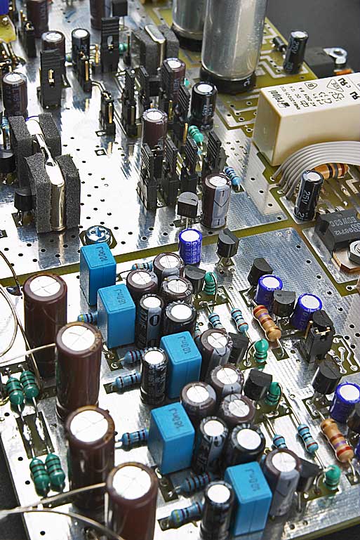


Galvanic Ground IsolationAfter every effort is made to ensure that the power supply is as free from high frequency interference as possible, it is important to draw our attention to the inner workings of the schematics themselves. Here, too, because of the potential interaction of the digital and analogue schematics, care must be taken to ensure that we encounter no loss of quality. Because LessLoss strives to achieve only the best possible solution, care is taken to separate the digital ground from the analogue ground. This is necessary because the digital input portion of a DAC acts as a mini transmitter of high frequency electromagnetic radiation. Not due to design, but due to the inherent properties of the high frequencies themselves.
Electrically and Galvanically Isolated GroundsAlthough many DAC designers are most likely aware of the issues involved in ground contamination by high frequency devices, often times these aspects are deemed too costly to overcome, and, hence, they are either ignored or dealt with in insufficient ways. As in the concept of battery power, LessLoss seeks the solution deeming the highest quality performance. This solution is found in electrically and galvanically isolating the digital and analogue grounds from each other. Only the rarest DAC design of high cost and commitment incorporate such a solution. Perhaps only two such manufacturers exist. High Frequency Radio vs. Low Frequency AudioThe digital input section contains a lowest jitter high frequency oscillator running at several MHz. This high frequency behaves differently than a low frequency audio signal. Every milimeter of distance that such high frequencies travel, and every component or voltage that these frequencies pass by locally on their way around the circuit influence them. In turn, they also influence their surroundings, in effect acting as radio transmitters propagating this signal. Because this frequency is desired at one, and only one location within the analogue schematics, care must be taken to isolate it at every twist and turn it takes. In the DAC 2004, you can see the transitional section between the digital and analogue schematics clearly. Please do not confuse our solution with the typical solution of simply putting the digital schematics on their own circuit board and connecting the various circuit boards with a bus-type cable. This is one of the worst Jitter-inducing methods since the bus is an antenna. That's why one sees various player upgrades with aluminum foil or copper foil covering the bus connections. The best method is not to incorporate this lossey distance into the design in the first place. In the LessLoss solution, both the digital and analogue circuits are on the same circuit board. There is no electrical or galvanic connection between the two, deeming the least ground contamination in the analogue circuitry. |
- Products
- Power Cables
-
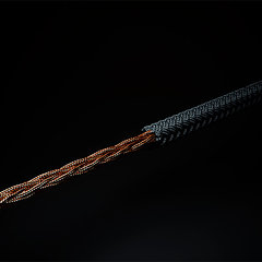
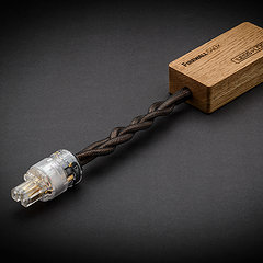
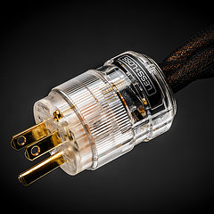 C-MARC™ Prime
The must have foundation for any sound system today.
From
$
486
C-MARC™ Prime
The must have foundation for any sound system today.
From
$
486
-
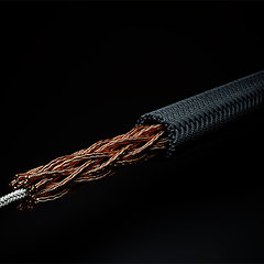
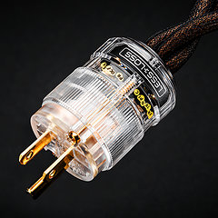
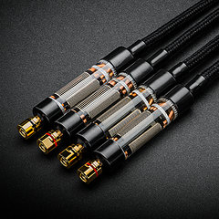
C-MARC™ Classic
The unique super-cable power cord everyone's talking about.
From
$
1148
-
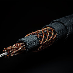
 C-MARC™ Classic Entropic Process
The peerless, advanced Classic masterpiece.
From
$
1934
C-MARC™ Classic Entropic Process
The peerless, advanced Classic masterpiece.
From
$
1934
-
C-MARC™ Stellar Entropic Process
The crown jewel for highest performance power connection.
From
$
2450
-
- Loudspeaker Cables
- Interconnect Cables
-
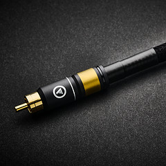
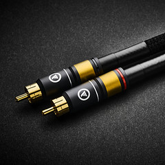 RCA C-MARC™
Cotton-clad true Litz • Whopping 2.3mm2 polarities
From
$
850
RCA C-MARC™
Cotton-clad true Litz • Whopping 2.3mm2 polarities
From
$
850
-
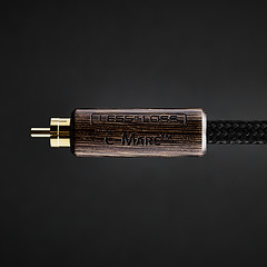
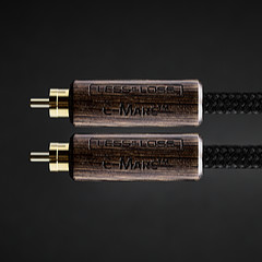 RCA C-MARC™ Entropic Process
Our finest RCA cable • Polished Wenge barrels
From
$
1428
RCA C-MARC™ Entropic Process
Our finest RCA cable • Polished Wenge barrels
From
$
1428
-
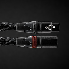 XLR C-MARC™
A hand-braided cotton-clad unique Litz construction
From
$
950
XLR C-MARC™
A hand-braided cotton-clad unique Litz construction
From
$
950
-
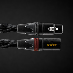 XLR C-MARC™ Entropic Process
Stratospheric performance for the audio connoisseur
From
$
1615
XLR C-MARC™ Entropic Process
Stratospheric performance for the audio connoisseur
From
$
1615
-
- Digital Cables
-
 RCA Digital C-MARC™
Cotton-clad unique Litz design • Made only by LessLoss
From
$
510
RCA Digital C-MARC™
Cotton-clad unique Litz design • Made only by LessLoss
From
$
510
-
 RCA Digital C-MARC™ Entropic Process
Possibly the most subtle digital cable on the planet
From
$
858
RCA Digital C-MARC™ Entropic Process
Possibly the most subtle digital cable on the planet
From
$
858
-
 XLR Digital C-MARC™
Featuring a whopping 3 x 2.3mm2 Litz construction
From
$
570
XLR Digital C-MARC™
Featuring a whopping 3 x 2.3mm2 Litz construction
From
$
570
-
 XLR Digital C-MARC™ Entropic Process
Stratospheric performance for the audio connoisseur
From
$
969
XLR Digital C-MARC™ Entropic Process
Stratospheric performance for the audio connoisseur
From
$
969
-
- Grounding Cables
- Bulk Wire and Cable
- Signal Conditioners
-
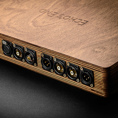
 Firewall for Loudspeakers
C-MARC™ Plug-and-Play Speaker signal conditioning like you've never imagined From $ 1656 -
 Firewall for Loudspeakers
DIY version for Self-Installation For the Do-It-Yourself project enthusiast • Solder yourself From $ 800 -
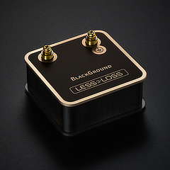 BlackGround DIY
Voltage-ground interface for a variety of applications
From
$
446
BlackGround DIY
Voltage-ground interface for a variety of applications
From
$
446
-
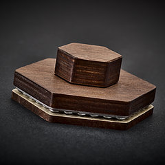
 BlackGround 8x/10x Speaker Base
Plug-and-play loudspeaker signal conditioner
From
$
3096
BlackGround 8x/10x Speaker Base
Plug-and-play loudspeaker signal conditioner
From
$
3096
-
- Power Conditioners
-
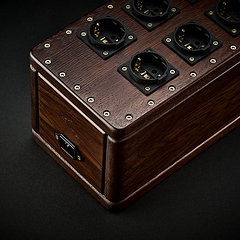
 Firewall 640x
Plug-and-play solution for any powered gear
Firewall 640x
Plug-and-play solution for any powered gear
C-MARC™ Entropic Process and standard lead versions From $ 654 -
 Firewall 640x DIY for Self-Installation
Self-solder and save!
From
$
320
Firewall 640x DIY for Self-Installation
Self-solder and save!
From
$
320
-
BlackGround DIY
Voltage-ground interface for a variety of applications
From
$
446
-
BlackGround 6x/10x Power Base
Plug-and-play power conditioner
From
$
2350
-
- Power Distributors
- Equipment Feet
- Field Conditioner
- DACs
- Power Cables
- Contact Us